
If your hardware engineering team is still designing printed circuit boards (PCBs) based on basic trace routing connectivity and treating end-of-line EMI filters as a lifesaver, your product will almost certainly fail when entering an anechoic chamber. Radiofrequency regulatory bodies such as the FCC (US), VCCI (Japan), or European market surveillance units do not accept forced, reactive fixes like wrapping extra copper tape or snapping on emergency ferrite beads, which only inflate mass production costs.
Electromagnetic interference does not generate out of nowhere, nor does it vanish on its own—it is the direct consequence of poor current return path management and unintended parasitic antenna designs right on the circuit board.
The High-Frequency Electromagnetic Reference Frame: Electromagnetic waves do not travel through copper traces; they travel in the dielectric substrate between the signal trace and the ground plane (GND Plane). If a high-speed signal line (Clock, Data Bus) crosses a split in a ground plane, a ground loop is immediately created. This transforms your PCB into an illegal radiation antenna that breaches the 30MHz−1GHz regulatory limits of the EN 55032 standard.
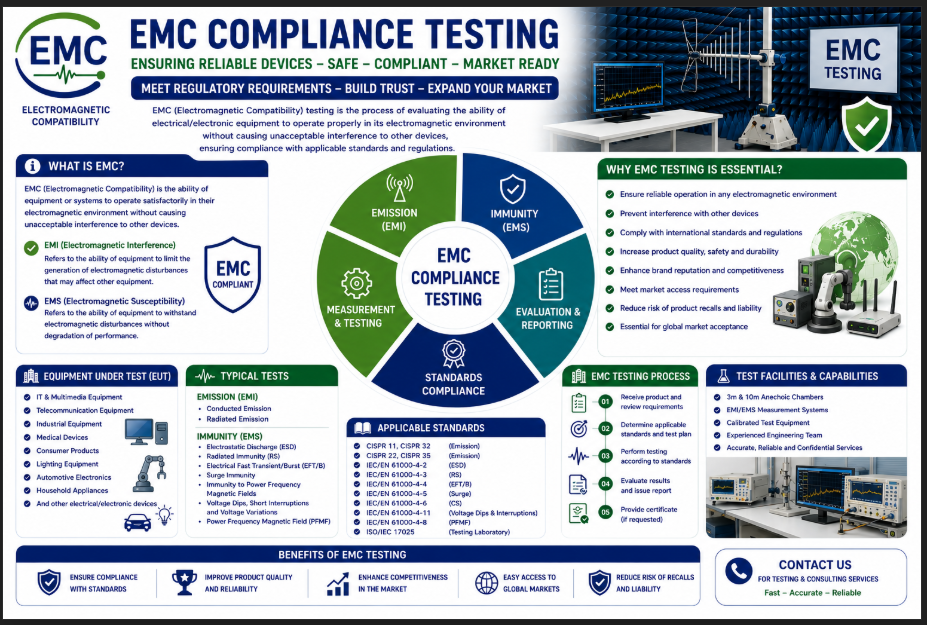
For Chief Technology Officers (CTOs) and Hardware Architecture Specialists, mastering EMC testing and suppression is the core capability of managing electromagnetic tolerances to preserve signal integrity.
1. Experimental Bottlenecks: Component Placement Blind Spots Privately Triggering Noise Radiation
Through practical debugging campaigns in testing labs, we have isolated 3 classic layout design flaws that cause hardware devices to fail immediately within the first few minutes of frequency spectrum scanning:
- Noise Leakage from the Switched-Mode Power Supply (SMPS): Power semiconductors (MOSFETs, Diodes) switching at high frequencies generate immense dV/dt and dI/dt voltage and current transients. If the layout fails to keep this current loop as compact as possible, this energy parasitically couples into adjacent signal lines, creating conducted emission noise that dumps back into the public utility grid.
- Signal-Layer Electrostatic Discharge Vulnerability (ESD Coupling): Designing discharge paths from the metallic enclosure or peripheral I/O ports (USB, HDMI, LAN) without proper isolation from the digital ground (Digital GND). When hit with an 8kV air ESD strike on the chassis, the surge current bypasses safe ground routing and discharges straight into processing chips (MCU/SoC), causing system lockups or hardware destruction.
- Inadequate Radiated Susceptibility Margin (RS Vulnerability): Small-signal analog measurement circuits lack localized shielding or common-mode chokes. When entering EMS testing and being bombarded by external radiofrequency fields (3V/m or 10V/m), the signal lines warp, forcing the device to log erroneous data and trigger automated system shutdowns.
The consequence is a rejected compliance report, a stalled project timeline, and the cancellation of shipping schedules just to restart the hardware lifecycle from scratch: spinning a new PCB—a process that burns thousands of dollars and misses critical market launch windows.
2. Technocratic Solutions: Restructuring the Ground Plane Matrix and Digitizing Pre-Compliance
To put an end to the trial-and-error design method, we establish a multi-layered electromagnetic defense framework, intervening deep within the hardware architecture via 4 technical tollgates:
- PCB Layer Stack-up Optimization: Establishing a multi-layer PCB architecture with continuous ground and power planes positioned immediately adjacent to signal layers to eliminate loop areas, forcing opposing electromagnetic fields to cancel each other out.
- Pre-compliance Scanning via Spectrum Analyzers: Deploying H-field and E-field near-field probes alongside spectrum analyzers in the local R&D lab to scan the board’s surface. This allows engineers to “see” the exact coordinates of peak emissions and resolve hot spots prior to final manufacturing runs.
- Independent Certification in a 10m Anechoic Chamber: Coordinating official certification tests inside standardized ISO/IEC 17025 accredited compliance labs, obtaining legally binding EMC (Emission & Immunity) test reports recognized globally.
- Digitization of the EMC Technical File: Packaging schematic diagrams, layout geometries, frequency spectrum logs, and data sheets of protective components (TVS Diodes, Ferrite Beads) into a centralized EMC Technical File, ready to fulfill technical audits from global buyers.
3. Performance Analysis: Insulating Cost Structures via Root-Cause Interference Suppression
Experimental history proves that investing engineering hours into noise suppression during the schematic and layout phases yields a massive financial advantage compared to patching errors post-production:
| Technical Parameters | Root-Cause Electromagnetic Management | Reactive Post-Design Patching |
|---|---|---|
| Bill of Materials (BOM Cost) | Cuts mass production costs by 8% to 12% by optimizing trace paths and eliminating expensive, unnecessary metal shields or heavy chokes. | BOM costs spike due to forcing extra capacitors, inductors, and expensive magnetic absorbing sheets onto the board to pass the lab. |
| First-Pass Lab Success Rate | Achieves a >95% pass rate during the first official compliance run, cutting testing lead times down to a few days. | Repeatedly fails lab evaluations, forcing multiple PCB revisions, stacking up chamber rental fees, and delaying shipping by months. |
| Circuit Reliability & Warranty Rate | High electromagnetic immunity keeps equipment operating reliably in harsh industrial environments, lowering field failure rates below 0.1%. | Devices experience random lockups, self-resets, or power failures from grid surges or environmental RF noise, inflating warranty expenses. |
4. 4-Step Action Roadmap: Structured Deployment from Schematic to Mass Production
Our EMC engineering protocol is deployed in phases to match the manufacturer’s hardware development milestones:
- Step 1 – Layout Audit & Electromagnetic Simulation: Reviewing the complete Gerber design, verifying clearance requirements, high-speed current paths, and the power distribution network (PDN).
- Step 2 – Experimental Pre-testing & Debugging: Running ESD strikes and near-field emission scans on early-stage prototypes, tuning filtering component values to secure a safety margin of at least 6dB below regulatory limits.
- Step 3 – Official Certification at an ISO 17025 Lab: Placing the product inside a standardized anechoic chamber, running firmware test routines at maximum workload configurations to secure official EMC compliance reports.
- Step 4 – Mass Production Quality Locking: Synchronizing incoming quality control tolerances for suppressive components (filters, chokes) and enclosure grounding fixtures on the assembly line to ensure absolute mass-produced consistency.
5. Merging Real-World ESG Targets with Electromagnetic Technocracy
Mastering electromagnetic compatibility benchmarks serves as definitive proof of an enterprise’s execution of its ESG (Environmental, Social, Governance) directives at an elite engineering level:
- The Social Pillar (Social): Restricting emission noise preserves the shared radiofrequency spectrum, ensuring that neighboring emergency communications or medical equipment are not jammed, fulfilling the highest baseline of public safety.
- The Environmental Pillar (Environment): Elevating electromagnetic susceptibility (EMS) protects devices against power grid instability, extending the physical and electronic lifespan of the product and directly minimizing e-waste.
- The Governance Pillar (Governance): Replacing bureaucratic compliance box-checking with transparent, empirical wave-field data and full adherence to international spectrum laws eliminates legal liabilities and builds equity with major institutional investors.
Conclusion
EMC testing and optimization has evolved past a simple administrative compliance item. It is a high-stakes engineering race centered on wave-field energy management and high-frequency hardware design.
Securing a clean circuit architecture and mastering the frequency spectrum provides your enterprise with a definitive shield for your export revenue. It strips away technical trade barriers in developed economies and positions your brand as a sustainable, top-tier technology vendor in the global value chain.
Contact us today to receive dedicated advice and the most suitable solution for your business!
Hotline: +84 933096426 – +84 868 591 260
Email:
Website:
Partners in Vietnam:
Contact Vietnam representative: Duc Luong Services
Hotline: +84 933096426 – +84 868 591 260
Email: ducluongservices@gmail.com
Website:
STC VN Co., Ltd.
Hotline: +84 933096426 – +84 868 591 260
Email: info@staunchlyservices.com.vn
Website: https://stauchlyservices.com.vn


No responses yet